This Ciber Lab was looking for ways to overcome limitations of volume and size, and to produce and reproduce nano-optical images more easily and at larger scales. The novelty they proposed was to move away from a process of fabrication that structurally bound image and material, to one that divided the material and the process. This would open the door to producing both small batches and larger images.
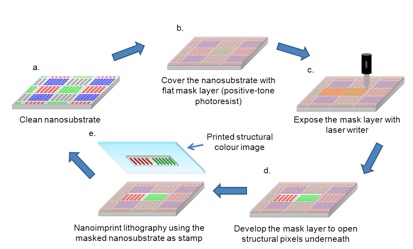
They developed a two-step approach (Fig. 1): 1) the production of a generic pixelated nanosubstrate, and 2) the accompanying processes for adding information onto/into it through an intensity control layer (ICL) or mask, which would individually control the luminance of the underlying RGB pixelated layer to make possible fully colourful images. Together these make up the lab’s central scientific contributions in terms of their retooling of the processes used for the production of nano-optical images and structures, which they to came to call nano media.

The generic nanosubstrate is made up of approximately one billion nanostructures in a square centimetre. These nano-hole arrays (NHAs) are produced using varying techniques, such as electron beam lithography (EBL) or focused ion beam (FIB) milling. Importantly, this system of NHAs is designed as a pixelated pattern using three (red-green-blue) or four (RGB + infrared) sub-pixels (see gallery). These are determined by the particular size and shape of the nanostructure so that, in the case of the information in the visible spectrum, the designated colour can be seen at a specific viewing angle.
Resolution meanwhile is defined based on the size and density of the NHAs and can differ according to the design of the pixelation pattern (e.g. bands or squares) and the materials used. In principle, a variety of materials can be pixelated in such a way, including metals, polymers, paper, tissue/fabric, or glass, and then coated through a process of metallization with silver, aluminum, or gold to brighten the colours (making use of the particular interactions of light with metal, or plasmonics).
A nano-optical substrate is not limited to the production of red, green, and blue colours. The idea of a generic pixelated canvas means that it can function much like a LCD screen. Rather than being electrically activated however, the pixels can be tuned through various mechanical or chemical processes to produce specific colours across the visible spectrum. The various methods for “tuning,” or patterning, the substrate—inscription, etching, exposing, writing, layering, molding, stamping, etc.—remediate the processes and logics of analog modes of image-making onto a new material, each coming with particular production or reproduction dis/advantages, and each resulting in a different quality of image.
In our projects, the image—including their colours, visibility angles, and brightness—had to be defined between the artists and scientists. Then, the Ciber Lab fabricated a master stamp according to this established design for each colour image. Then, secondary stamps with generic pixel bands (in R, G, B) were replicated from the master stamp and “tuned” using micro-scale patterning techniques, including optical lithography, photographic recording, inkjet printing, or laser writing (chosen based on the required resolution and colour levels of the final image produced).

Figure 1 shows one typical process where a secondary stamp is patterned using optical lithography to define a specific structural colour pattern. The generic substrate is first coated with a photosensitive material, which can be selectively removed using optical lithography. Optical lithography can be done using either UV laser writing or UV exposure through a binary photomask. With exposure followed by chemical development, here the nano-structures were selectively opened and replicated onto another separate substrate which became the final colourful nano media artefact.
As the Lab’s techniques of “addition” developed or shifted, a variety of terms were floated about in the team to describe this nano-optical visual technology: nanographs, nanophotos, nanoprints, nanofilm, nano-etchings. The familiar ring to these names was no coincidence as the material process of adding an image to a substrate follow the same logic as analog methods for producing images, and these processes did serve as inspirations for the scientific team.

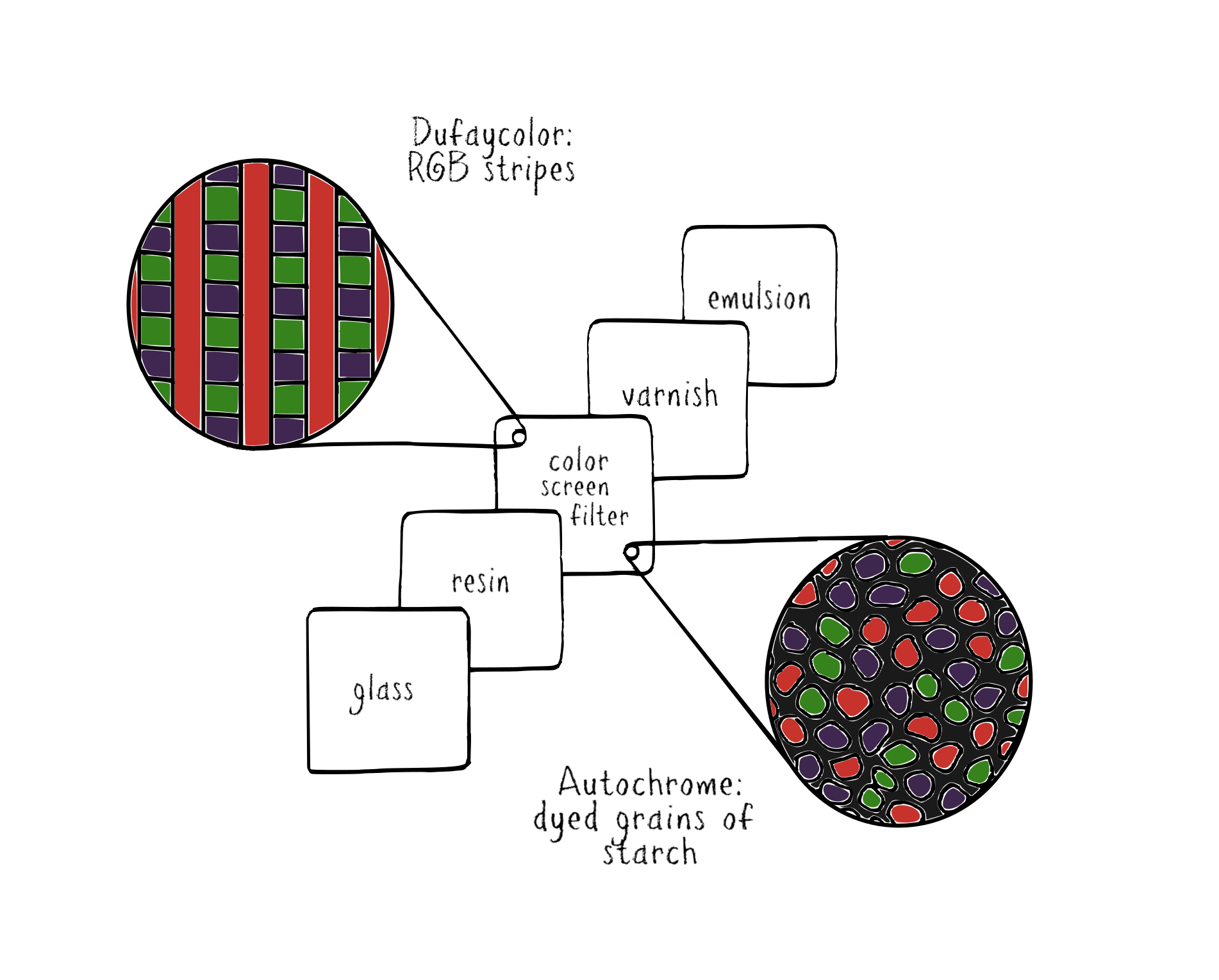
The histories of printed pictures, photomechanical processes, and screen technologies allow us to see the many ways that nano-optical image-making can be mapped onto the technical histories of art and media production. Processes from the early 20th century like Dufay colour film or autochromes (Fig. 1), for example, used a similar principle that relied on a generic pixelated pattern made up of the additive primaries—red, green, blue—and a coating system (in these cases, black-and-white) for modulating the colours as desired. Later, photographic emulsions with separated coloured layers became the dominant colour recording medium. The scales and materials have changed, but the basic principles of how to work with light to fix colours and pictures has remained. And this without even yet considering the infrared subpixel, which reminds us that a nano-optical material can also store information invisibly, ultimately encoding information through a system of grooves, pits, and holes much like it has been done in punched card systems or optical discs.
Here is documentation of the fabrication process of Nano Media at Ciber Lab.
Hi. I'm popup. I contain additionnal information about this.
Hi. I'm popup. I contain additionnal information about this.
Hello. Welcome into Project Nanoverse. Nice to meet you!