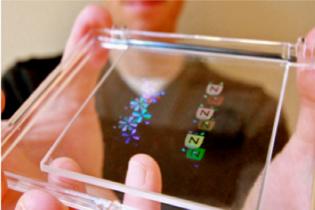

Engineering scientists, inspired by the iridescence occurring in nature, are now designing materials that can mimic these nanoscale mechanism and effects (these are sometimes called metamaterials). While the morpho butterfly’s specific structure produces perceivable colours in the blue range, engineers can design a variety of nano-sized structures such as holes or slits (“arrays”) in different materials to generate a wide range of precise colours and “optical effects.” The resulting film-like substrates, supports for a new kind of visual experience, are what Giuliana Bruno might refer to as a new “fabric of the visual” [1].
Some artists have experimented with nano-optical materials, producing objects that function much like prisms [2]. But one of the challenges in working with nano-optical materials has been not just a general production of structural colour in and of itself, but specifically to fine-tune the design of the nano-structures enough as to be able to produce distinct “high-definition” images. Here the nano-optical substrate “contains” images (and information) in its structure. But the most advanced domain for this material is not in art, but rather security printing…

This production of materials with nano-optical effects has, to date, been largely the domain of the security printing industry, which uses it to produce visual authentication devices for objects such as money and official documents like passports. These are examples of a new generation of what are described as optical variable devices (OVDs). OVDs are characterized by their changeability, or iridescent visual effects. One common OVD is the holograph, but nano-OVDs are produced using a different technical principle: whereas holographs are based on the recording, or inscription, of a whole image on a holographic film (substrate) with reflected laser light, the nano-OVD’s visual effect relies on structural colour. In general, the advantages of images that use structural colour instead of pigments is their resistance to fading and their longevity—both useful for securing documents—and the ability to produce tuneable luster [Ref. J6].
The typical way of producing nano-OVDs as an anti-counterfeit device is through renewals of familiar techniques—lithography, embossing, stamping. First, a master of a wanted image is fabricated (the “original”) in a nickel stamp (using nanolithography), which is then replicated through roll-to-roll embossing in a colorless polymer/plastic. For each new image, a new master stamp must be produced with the optical image structurally integrated into the material: the colour from each hole of the nanosubstrate is a direct outcome of the stamping process. This technique means that to reproduce is to make a copy of a combined material-image each time, which poses challenges both in terms of volume and size. Using this method means that it only makes sense to produce small images that need to be copied many times over, making the production of many different images in small quantities or in large format impractical or unfeasible.

Hi. I'm popup. I contain additionnal information about this.
Hi. I'm popup. I contain additionnal information about this.
Hello. Welcome into Project Nanoverse. Nice to meet you!